Historical Development
- Origins: The electron microscope was developed in the early 1930s by German engineers Ernst Ruska and Max Knoll, who built the first transmission electron microscope (TEM) in 1931.
- Technical breakthrough: The theoretical foundation came from Louis de Broglie’s 1924 hypothesis that electrons possess wave-like properties, providing the potential for much higher resolution than light microscopy.
- Commercial development: The first commercial electron microscope was manufactured by Siemens in 1939, revolutionizing scientific imaging capabilities.
- Evolution: Subsequent decades saw tremendous improvements in electron microscope design, resolution capabilities, and specialized applications, leading to multiple Nobel Prizes related to the technology.
Basic Principles of Electron Microscopy
- Wave-particle duality: Electrons behave both as particles and waves, with wavelengths approximately 100,000 times shorter than visible light, enabling vastly superior resolution.
- Electron generation: A heated filament (usually tungsten) emits electrons through thermionic emission in a vacuum environment.
- Acceleration: These electrons are accelerated by an electric field, typically at voltages between 100-300 kV (kilovolts).
- Electron lenses: Electromagnetic coils function as “lenses” to focus the electron beam, similar to how glass lenses focus light in optical microscopes.
- Beam-specimen interaction: When electrons interact with a specimen, various signals are produced (transmitted electrons, backscattered electrons, secondary electrons, X-rays, etc.) that can be detected to form images or provide analytical information.
- Resolution advantage: While light microscopes are limited to about 200 nanometers resolution by the wavelength of visible light, electron microscopes can achieve resolution below 0.1 nanometers.
Major Types of Electron Microscopes
Here’s a comparative table of the main types of electron microscopes:
| Type | Full Name | Working Principle | Typical Resolution | Sample Requirements | Primary Applications |
|---|---|---|---|---|---|
| TEM | Transmission Electron Microscope | Electrons pass through an ultra-thin specimen | 0.05-0.2 nm | Ultra-thin sections (<100 nm) | Internal cellular structures, crystal structures, nanomaterials |
| SEM | Scanning Electron Microscope | Electron beam scans surface; secondary electrons create image | 1-20 nm | Conductive surface coating, minimal preparation | Surface topography, material composition, failure analysis |
| STEM | Scanning Transmission Electron Microscope | Combines TEM and SEM principles; focused beam scans through sample | 0.05-0.1 nm | Ultra-thin sections | Atomic-resolution imaging, element mapping |
| Cryo-EM | Cryogenic Electron Microscope | TEM variant where samples are flash-frozen | 0.2-0.3 nm | Flash-frozen samples | Biological structures in native state, protein structure |
| FIB | Focused Ion Beam | Uses ions instead of electrons for imaging and milling | 5-10 nm | Various | Sample preparation, circuit modification, 3D tomography |
Components of an Electron Microscope
- Electron source: Provides the electron beam, typically using:
- Tungsten filament (simplest, least expensive)
- LaB₆ (lanthanum hexaboride) crystal (brighter, longer-lasting)
- Field emission gun (highest brightness, best resolution)
- Vacuum system: Essential to prevent electrons from scattering off air molecules, typically maintaining pressures of 10⁻⁴ to 10⁻¹⁰ torr.
- Electromagnetic lenses:
- Condenser lenses: Control beam intensity and spot size
- Objective lens: Forms the initial image
- Projector lenses: Magnify the image further (in TEM)
- Specimen stage: Precisely positions the sample in the electron beam path, often with capabilities for tilting, rotating, and heating/cooling.
- Detectors: Convert electron signals into viewable images through:
- Fluorescent screens
- Photographic plates (historically)
- CCD (charge-coupled device) cameras
- Direct electron detectors (newest technology)
- Computer systems: Control microscope parameters and perform image processing, analysis, and reconstruction.
Transmission Electron Microscope (TEM)
- Working Principle: Electrons pass through an ultra-thin sample, creating a 2D image based on the varying electron absorption or scattering by different parts of the specimen.
- Key Components:
- Electron gun (electron source)
- Condenser lenses (focus the electron beam)
- Specimen stage
- Objective lens
- Projector lenses
- Imaging system (fluorescent screen or digital detector)
- Magnification Range: Typically 500x to 1,500,000x
- Applications:
- Cellular ultrastructure in biology
- Crystal structure analysis in materials science
- Virus and protein structure determination
- Semiconductor device inspection
- Limitations:
- Requires extremely thin specimens
- Sample preparation is complex and can introduce artifacts
- Limited field of view
- Electron beam can damage delicate biological specimens

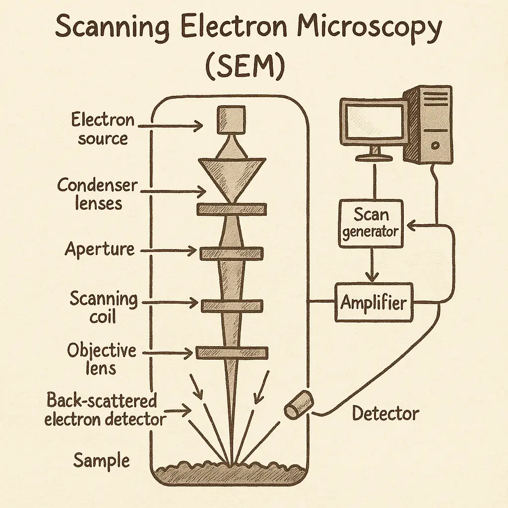
Scanning Electron Microscope (SEM)
- Working Principle: A focused electron beam scans the specimen surface, with detectors capturing various signals (particularly secondary electrons) to create a 3D-like image.
- Key Components:
- Electron gun
- Electromagnetic lenses
- Scanning coils
- Secondary electron detector
- Backscattered electron detector
- X-ray detector (for elemental analysis)
- Magnification Range: Typically 10x to 300,000x
- Applications:
- Surface topography analysis
- Failure analysis in engineering
- Forensic investigation
- Geological sample characterization
- Archaeological artifact examination
- Advantages Over TEM:
- Greater depth of field
- Easier sample preparation
- Larger specimens can be examined
- 3D-like imaging capabilities
Sample Preparation Techniques
- TEM sample preparation:
- Ultramicrotomy: Cutting ultra-thin sections (50-100 nm) using diamond knives
- Ion milling: Thinning samples using argon ions
- FIB sectioning: Precise cutting with gallium ion beams
- Chemical thinning: Using acids or other chemicals to thin samples
- SEM sample preparation:
- Dehydration: Removing water to prevent vacuum issues
- Coating: Applying conductive materials (gold, platinum, carbon) to prevent charging
- Critical point drying: Preserving structure during dehydration
- Freeze-drying: Alternative to chemical fixation
- Cryo-preparation:
- Plunge freezing: Rapidly immersing specimens in liquid ethane
- High-pressure freezing: Applying pressure during cooling to prevent ice crystal formation
- Freeze-substitution: Replacing ice with organic solvents at low temperatures
Image Formation and Interpretation
- Contrast mechanisms in TEM:
- Mass-thickness contrast: Areas with higher atomic number or thickness appear darker
- Diffraction contrast: Crystalline regions create contrast based on crystal orientation
- Phase contrast: Interference between electron waves creates high-resolution images
- Contrast in SEM:
- Topographic contrast: Surface features affect electron emission
- Compositional contrast: Elements with higher atomic numbers appear brighter
- Voltage contrast: Electrically charged regions appear different
- Artifacts and limitations:
- Beam damage: Electron irradiation can alter or destroy specimens
- Charging: Accumulation of electrons on non-conductive samples
- Contamination: Carbon deposition during imaging
- Sample deformation: Preparation or vacuum exposure can alter native structure
Advanced Electron Microscopy Techniques
- Analytical techniques:
- Energy-dispersive X-ray spectroscopy (EDS): Identifies and maps elements
- Electron energy loss spectroscopy (EELS): Analyzes energy transferred to samples
- Electron diffraction: Determines crystal structures and orientations
- Three-dimensional methods:
- Electron tomography: Creates 3D reconstructions from tilt series
- FIB-SEM: Sequential milling and imaging for 3D analysis
- Serial block-face imaging: Automated sectioning and imaging
- In-situ techniques:
- Liquid-cell EM: Observes specimens in liquid environments
- Heating/cooling: Studies temperature-dependent processes
- Mechanical testing: Observes deformation under stress
- Environmental EM: Examines samples in gas environments
Applications Across Scientific Fields
- Materials science:
- Nanostructure characterization
- Defect analysis in crystals
- Interface and grain boundary studies
- Failure analysis in engineering materials
- Biological sciences:
- Cellular ultrastructure investigation
- Protein structure determination
- Virus morphology studies
- Tissue pathology
- Semiconductor industry:
- Quality control in chip manufacturing
- Failure analysis
- Process optimization
- Nanolithography
- Forensic science:
- Gunshot residue analysis
- Fiber examination
- Document authentication
- Trace evidence analysis
- Environmental studies:
- Particulate pollution characterization
- Microplastic analysis
- Soil mineral composition
- Nanomaterial environmental impact assessment
Comparison with Other Microscopy Techniques
| Technique | Resolution Range | Sample Requirements | Advantages | Limitations |
|---|---|---|---|---|
| Light Microscopy | ~200 nm | Minimal preparation, living specimens possible | Simple preparation, color imaging, live cell observation | Limited resolution, low depth penetration |
| Electron Microscopy | 0.05-20 nm | Vacuum-compatible, often fixed/dehydrated | Extremely high resolution, analytical capabilities | Complex sample prep, no living specimens, grayscale images |
| Atomic Force Microscopy | 0.1-10 nm | Surface accessibility | 3D topography, mechanical properties, ambient conditions | Slow scanning, limited to surfaces |
| X-ray Microscopy | 10-100 nm | Minimal preparation | Penetrates thick samples, minimal preparation | Lower resolution than EM, limited contrast |
| Super-resolution Light Microscopy | 20-100 nm | Fluorescent labeling | Living specimens, color, specific labeling | Complex setup, limited to fluorescent structures |
Current Challenges and Future Directions
- Technological challenges:
- Reducing beam damage to sensitive specimens
- Improving detector sensitivity and speed
- Enhancing automation and throughput
- Developing better in-situ capabilities
- Emerging techniques:
- 4D STEM: Captures diffraction patterns at each scan position
- Ptychography: Computational phase reconstruction for higher resolution
- Integrated correlative microscopy: Combining EM with other imaging modalities
- Machine learning applications: Automated image analysis and reconstruction
- Future prospects:
- Atomic-resolution tomography of complex materials
- Dynamic imaging of molecular processes
- Integration with spectroscopic techniques for comprehensive analysis
- More accessible, lower-cost electron microscopy platforms
Economic and Practical Considerations
- Cost factors:
- Basic SEM systems: $100,000-$500,000
- Advanced TEM systems: $1-10 million
- Annual maintenance: 5-10% of purchase price
- Facility requirements: Vibration isolation, electromagnetic shielding, stable power
- Operational considerations:
- Trained operators required
- Sample preparation expertise needed
- Consumables (filaments, apertures, etc.)
- Data storage and processing requirements
- Shared facility models:
- Core facilities at universities and research centers
- Commercial analytical services
- Industrial research collaborations
Frequently Asked Questions
Q1: What’s the main difference between SEM and TEM? A1: SEM (Scanning Electron Microscopy) scans a beam across the sample surface to create images based primarily on electrons emitted from the surface, providing excellent 3D-like views of surface features. TEM (Transmission Electron Microscopy) passes electrons through an ultra-thin sample, creating images based on how electrons interact with and pass through the internal structure of the specimen, providing higher resolution views of internal structures.
Q2: Can electron microscopes see atoms? A2: Yes, high-resolution transmission electron microscopes (TEMs) and scanning transmission electron microscopes (STEMs) can visualize individual atoms, particularly in crystalline materials where atoms are arranged in regular patterns. Aberration-corrected electron microscopes have pushed resolution below 0.05 nanometers, allowing for routine atomic-resolution imaging.
Q3: Why are samples for TEM so thin? A3: TEM samples must be extremely thin (typically less than 100 nanometers) because electrons must be able to pass through the specimen to form an image. If samples are too thick, electrons will be completely scattered or absorbed rather than transmitted, resulting in no useful image formation.
Q4: Can living specimens be viewed with electron microscopes? A4: Generally no, conventional electron microscopy requires a high vacuum environment that would kill living organisms. Additionally, the electron beam itself causes significant damage to biological structures. However, specialized environmental SEMs can image some hydrated specimens under low vacuum conditions, and developments in liquid-cell technologies are advancing capabilities for observing specimens in near-native conditions.
Q5: How is color added to electron microscope images? A5: Electron microscopes inherently produce grayscale images because electrons don’t have color properties like photons (light). Colors in EM images are artificially added during post-processing, either for aesthetic purposes or to highlight different features, structures, or elemental compositions. In analytical techniques like EDS, colors often represent different chemical elements.
Q6: What’s the difference between resolution and magnification? A6: Magnification refers to how much larger an object appears compared to its actual size (e.g., 10,000×), while resolution refers to the smallest distance between two points that can be distinguished as separate entities. High magnification is useless without good resolution. Electron microscopes offer both high magnification (up to millions of times) and excellent resolution (down to atomic levels).
Q7: How long does it take to acquire an electron microscope image? A7: Image acquisition times vary widely depending on the technique, desired quality, and beam sensitivity of the sample. Simple SEM images might take seconds to acquire, while high-resolution, low-noise TEM images might require minutes of exposure. Advanced techniques like tomography or spectroscopic mapping can take hours to complete.
References and Further Reading
- Williams, D.B. & Carter, C.B. (2009). Transmission Electron Microscopy: A Textbook for Materials Science. Springer Science & Business Media
- Reimer, L. & Kohl, H. (2008). Transmission Electron Microscopy: Physics of Image Formation. Springer Series in Optical Sciences
- Goldstein, J. et al. (2017). Scanning Electron Microscopy and X-ray Microanalysis. Springer
- Journal of Microscopy. Wiley Online Library
- Microscopy and Microanalysis. Cambridge University Press
- Microscopy Today. Cambridge University Press
- Electron Microscopy Society of America. Official Website
- International Federation of Societies for Microscopy. Official Website
- De Jonge, N. & Ross, F.M. (2011). Electron microscopy of specimens in liquid. Nature Nanotechnology
- Dubochet, J. et al. (1988). Cryo-electron microscopy of vitrified specimens. Quarterly Reviews of Biophysics