Scanning Electron Microscope (SEM):
The Scanning Electron Microscope was developed by professor Dr. Charles Oatlev in the 1950s. Scanning Electron Microscope is useful for studying surface structures of thick specimens. The electrons do not form the image by being transmitted but by getting emitted from the surface of the specimen. It gives a typical three-dimensional appearance.
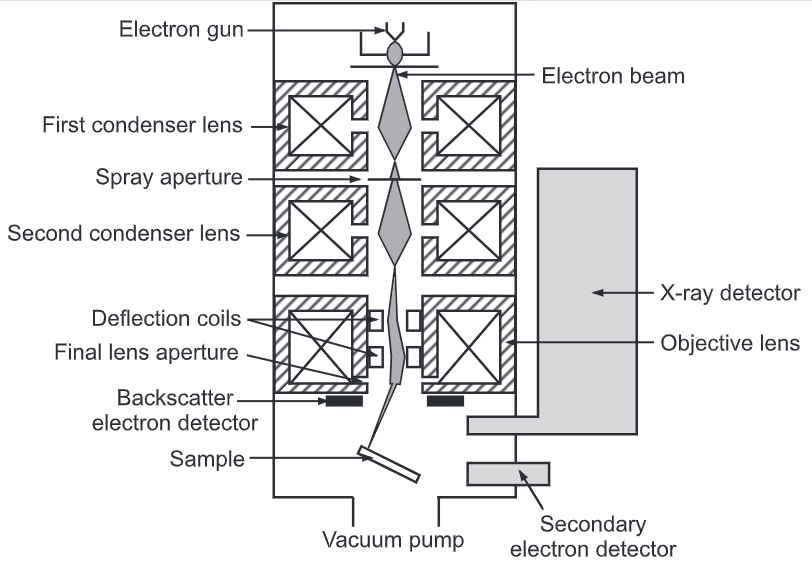
SEMs consist of the following components:
- Electron source
- Electron gun
- Electromagnetic and/or Electrostatic Lenses
- Vacuum chamber
- Sample chamber and stage
- Computer
- Detectors (one or more)
- Secondary Electron Detector (SED)
Image Forming:
The image forming process begins with an electron gun generating a beam of energetic electrons down the column and onto a series of electromagnetic lenses.
Samples are specially prepared by first undergoing dehydration and then being coated with a thin layer of a conductive material, such as gold. Living cells and tissues and whole, soft-bodied organisms require chemical fixation to preserve and stabilize their structure. Fixation is usually performed by incubation in a solution of a buffered chemical fixative, such as glutaraldehyde in combination with formaldehyde. Freeze-fracturing is a preparation method particularly useful for examining lipid membranes and their incorporated proteins in the “face on” view. The preparation method reveals the proteins embedded in the lipid bilayer.
The illuminating system of SEM is like TEM. The electron beam is compressed by using condenser coils which results in the formation of an electron probe, a narrow pencil of electrons. The electrons which fall on the object are primary electrons and which are emitted from the specimen are secondary electrons. The specimen is kept at an inclined angle. If the primary electrons enter a pit very few secondary electrons are emitted. The projected areas emit more secondary electrons. The three-dimensional image is formed by secondary electrons.
In SEM the secondary electrons are first collected amplified and then used for the formation of an image on the phosphor screen of a cathode ray tube (CRT). One cathode ray tube is used for visual observation of the specimen and the other is used for photography.
The SEM produces images by probing the specimen with a focused electron beam that is scanned across the specimen. When the electron beam interacts with the specimen, it loses energy by a variety of mechanisms. The lost energy is converted into alternative forms such as heat, emission of low-energy secondary electrons and high-energy backscattered electrons, light emission (cathodoluminescence), or X-ray emission, all of which provide signals carrying information about the properties of the specimen surface, such as its topography and composition.
Generally, the image resolution of an SEM is lower than that of a TEM. However, because the SEM images the surface of a sample rather than its interior, the electrons do not have to travel through the sample. This reduces the need for extensive sample preparation to thin the specimen to electron transparency.
SEM Applications:
- SEMs have a variety of applications in a number of scientific and industry-related fields, especially where characterizations of solid materials are beneficial.
- In addition to topographical, morphological, and compositional information, a Scanning Electron Microscope can detect and analyses surface’ fractures, provide information in microstructures, examine surface contaminations, reveal 3-D variations in chemical compositions, provide qualitative chemical analyses and identify crystalline structures.
- SEMs can be an essential research tool in fields such as life science, biology, geology, medical and forensic science, metallurgy.
- In addition, SEMs have practical industrial and technological applications such as semiconductor inspection, production line of minuscule products, and assembly of microchips for computers.
SEM Advantages:
- The detailed three-dimensional and topographical imaging and the versatile information garnered from different detectors.
- SEMs are easy to operate with the proper training and advances in computer technology and associated software make operation user-friendly.
- This instrument works fast, in addition, the technological advances in modern SEMs allow for the generation of data in digital form.
Limitations of electron microscopy:
- Cells can not be observed in their live state.
- Dehydration of specimen can cause ultrastructure defects.
- For TEM the specimen should be very thin.
- The cost of an electron microscope is very high.
- Specimen preparation is time-consuming
Difference Between TEM and SEM
| Character | TEM | SEM |
| Source of illumination | Electrons | Electrons |
| Type of electrons forming the image
| Transmitted electrons
| Secondary electrons reflected off the surface of the specimen |
| Medium of travel | High vacuum | High vacuum |
| Positioning of the specimen | Perpendicular to electron beam | In an inclined plane relative to electron beam |
| Specimen processing
| Staining/Shadow casting/ Freeze fracturing | Heavy metal (gold, palladium) coating |
| Type of Image formation | Two dimensional
| Three dimensional
|
| Type of screen for visualization | Fluorescent screen
| Phosphor screen of a cathode ray tube |
| Magnification | 500,000X to 1,000,000X | 10,000X to 1,000,000X |
| Resolution | 1.0 nm | 1.0 to 10.0 nm |
| Application | Study of cell ultrastructure | Study of cellular topography |
You May Read: Phase contrast microscopy: Definition, principle, parts, uses